Successful Cleaving of Delicate Nanostructures Fabricated Using E-Beam Lithography
"... we were able to spend less time preparing samples, with less wasted material in each run."
-Tommaso Pregnolato, Ph.D. Fellow
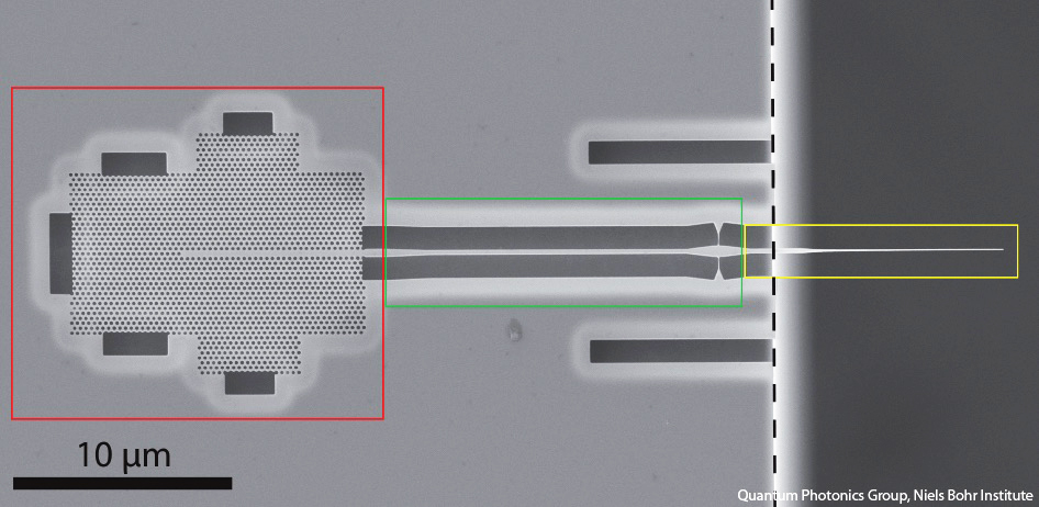
Learn how scientists in the Quantum Photonics Group at the Niels Bohr Institute of the University of Copenhagen who are developing new technologies for photonic and quantum-information applications used the LatticeAx to alleviate one of their biggest sample preparation challenges: precise cleaves on small samples without damaging delicate fabricated nanostructures.
As part of this research, the team has developed processes whereby they fabricate suspended photonic crystals and other nanostructures using GaAs. The nanostructures themselves are between 160 and 180 nm thick. To perform experiments on these structures, the team needed to be able to cleave small samples without damaging the small and delicate devices that they had fabricated. And they absolutely required a method that minimized sample handling to further reduce the potential for damage to the nanostructures.
Download the use case to learn more about how a successful process was developed to cleave these delicate fabricated samples.
Go online to learn more about the research being conducted in the Quantum Photonics Group at the Niels Bohr Institute, University of Copenhagen: http://quantum-photonics.nbi.ku.dk/
