Wafer Dicing
Wafer Dicing Applications and Tools
Automated dicing tools are great when used in production environments where large numbers of wafers are processed and the wafer and die dimensions are constant. During R&D and when only a small batch of die are required, it is beneficial to have clean, accurate, repeatable, and fast tool to dice wafers. Low cost and cost of ownership and ease of use are also key requirements during R&D.
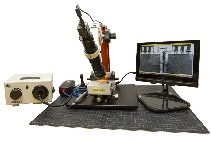
LatticeGear designs, manufactures, and sells cleanroom compatible benchtop tools for cleaving a wide variety of substrates, both crystalline and amorphous, including silicon, GaAs, InP, sapphire, and glass. Based on wafer composition, size (dimensions and thickness), and crystal orientation LatticeGear can recommend tools and a process to dice wafers. For an overview of the products and applications watch the video on the right.
Eagle XG Glass Substrate
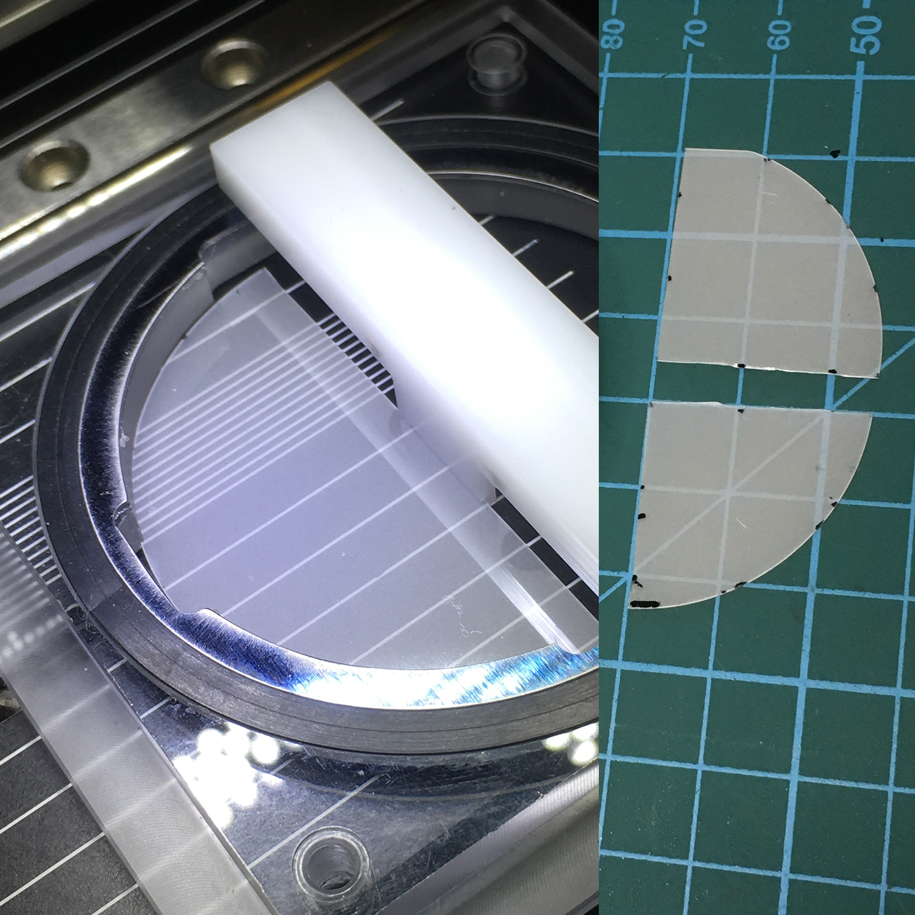
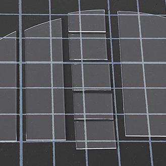
Eagle XG glass substrates used in the LCD industry were purchased to see whether the cleaving process could be modified to dice a 6" glass wafer. Using the FlexScribe and a diamond cutting wheel, followed by 3 point cleaving with the LatticeAx, the wafer can be cut cleanly without particulate contamination or fractures in unwanted directions. A three point cleave is achieved by creating pressure on a sample underneath the scribe and two pressure points on top of the sample, equidistance from the scribe.The image on the right shows the cleanliness of the cuts. The 1cm2 die were made by scribing with the FlexScribe and cleaving the samples with the LatticeAx which created clean, vertical facets.
Sapphire Wafer
On the right is a movie showing the use of the FlexScribe to scribe a 2" c-plane sapphire wafer. The wafer was marked prior to scribing. The process is quick and clean. In this example a the wafer was cleaved using the edge of the mat to create stress on the bottom side of the wafer.
Dicing a silicon wafer with the LatticeAx, FlipScribe and FlexScribe
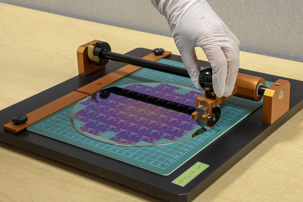
Dicing silicon wafers is very straight forward with the right tools. In the video below a 300 mm patterned silicon wafer was diced using the LatticeAx, FlipScribe and the FlexScribe. Choosing the right tool for the job is important and is based on the final outcome needed. Here are some basic guidelines:
- LatticeAx most accurate and clean solution because it creates a highly accurate indent (not a scribe) and has the cleaving mechanism integrated into the tool. The 3 pt cleaving system creates the cleanest, vertical mirror finish surfaces needed for SEM cross sections and photonics.
- FlipScribe backside scriber. No particles or damage generated on the frontside of the wafer as the scribe is made on the backside. Able to scribe glass and silicon 111 or off crystal axis as it can make short and long scribes. Cleaving with pliers or over pins and edges.
-
FlexScribe frontside scriber. Easy to use, fast, and can make short and long scribes. Configurable with a variety of cutting wheels to address very thin and hard materials. Creates few particles. It excels at cleaving glass and is a necessity when off crystal axis cleaving is required.
GaN Wafer Downsizing
For III-V substrates and wafers that are cubic such as GaAs and InP, brittle and relatively soft on the mohs hardness scale, cleaving is simple. The LatticeAx alone, does a great job downsizing these materials. It is clean, dry and fast.
For materials that are not cubic or need to be cleaved counter to a crystal plane, tools that can scribe across the entire length of the sample are required. Have a look at the Sapphire page for an explanation. You will need the FlipScribe or FlexScribe to make full length scribes and cleave wafers with hexagonal and trigonal structures. Examples of these materials are GaN, AlN, SiC and Sapphire.
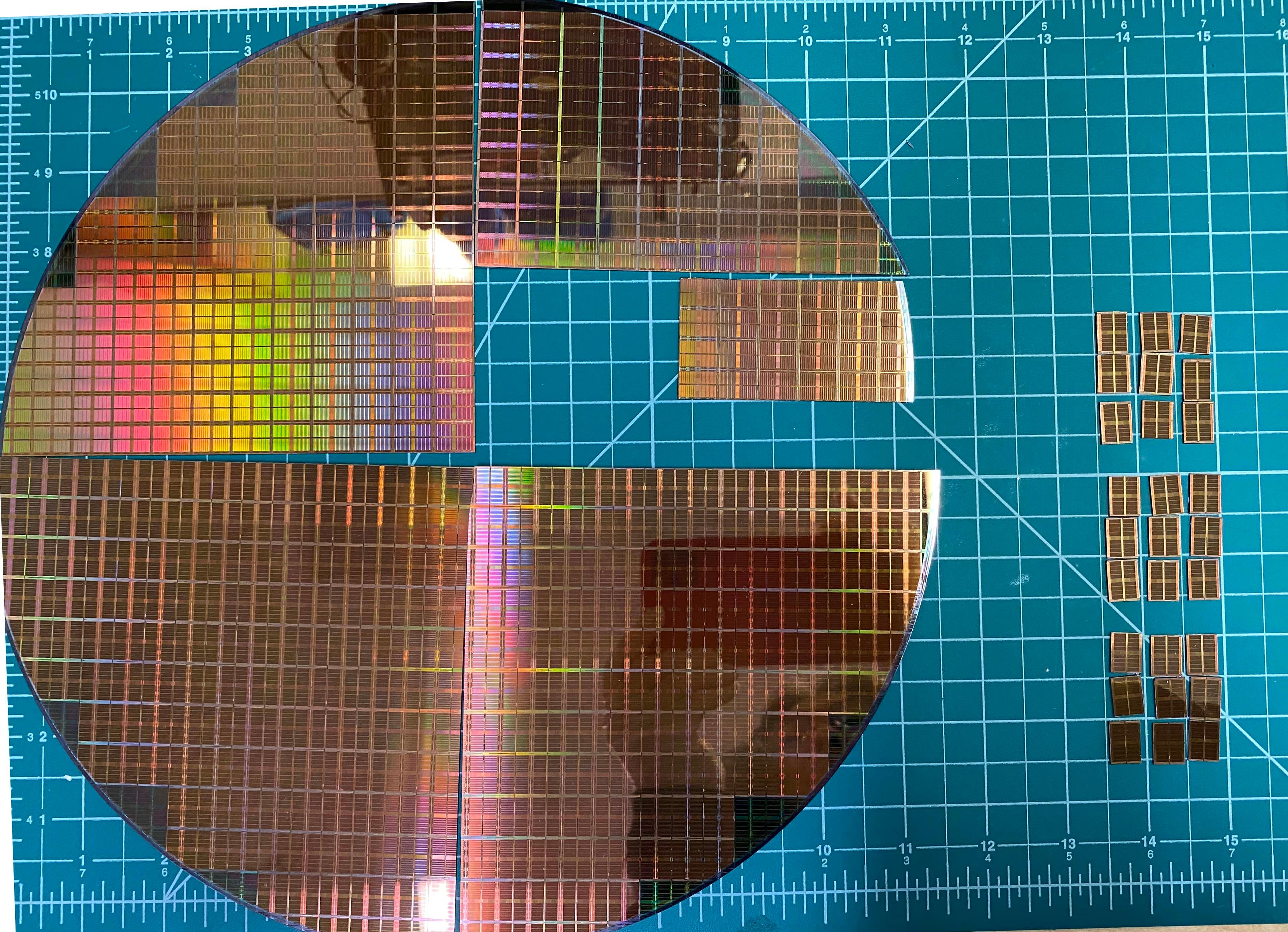
The images on the right are from a 2” GaN wafer. Scribing was done with the FlipScribe and the FlexScribe. The FlexScribe was used to downsize the whole wafer in half. The FlipScribe was used to further downsize by scribing the backside of the wafer, eliminating contamination to the top surface. The combination of frontside and backside scribing give the user flexibility to develop a process for wafers with non-cubic structures. Cleanbreak cleaving pliers were used after scribing to cleave.
Solutions
There are just a few things to think about when choosing tools for cutting glass.
- What is my substrate size and thickness?
- Do I need mirror finish edges (typically needed for photonics devices)?
- Do I want to cleave samples for cross section analysis by SEM?
The solution may require one or more tools to get the job done. For instance:
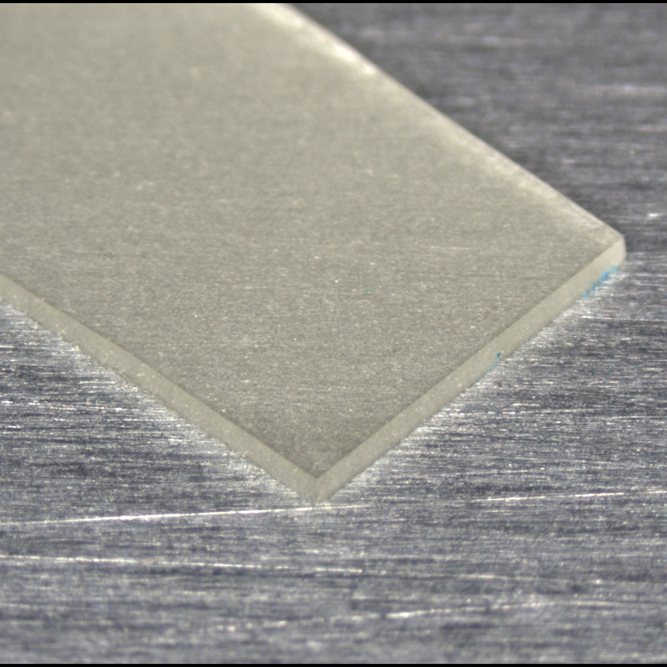
- For downsizing large thin (<200 micron) glass wafers into 1 cm2 die, no mirror finish required. Use the FlexScribe with PCD diamond cutting wheel.
- For preparing samples that must have mirror finish facets for photonics or SEM analysis. Downsize with the FlexScribe or FlipScribe and make the final cleave with the LatticeAx.
- Preparing samples that have sensitive thin films on the surface. Use the FlipScribe backside scriber to downsize the samples. Make the final cleave using the LatticeAx to obtain mirror finish facets.
Products for Wafer Dicing
Based on your application, LatticeGear can recommend the right tool set. Please CONTACT US!
Scribing and Cleaving Tools
There are a number of accessories and consumables that will be important for your laboratory.
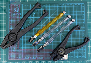
CleanBreak Pliers with 3 Sets of Jaws. After scribing you will need to cleave your sample. It is possible to cleave over a sharp edge but the pliers provide symmetrical force when breaking the glass. Cleanbreak pliers are used for samples 20mm/.75" and larger.
Videos
Watch videos showing the operation of the scribing and cleaving tools and systems.
Publications
Publications (for copies, contact lg@latticegear.com) or for downloadable copies of these publications you must be registered and signed in
